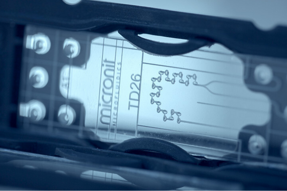
Wet Etching: Crafting Complex Patterns in Microfluidic Chips
Wet etching is a foundational manufacturing technique used to etch precise patterns into substrates like glass and silicon, crucial for microfluidic chip production. This process involves the controlled application of chemical solutions, such as hydrofluoric acid (HF) for glass and alkali hydroxides like KOH or TMAH for silicon. These chemicals meticulously remove material, following patterns defined by photolithography, to create intricate channels and structures. Wet etching can be isotropic, affecting the substrate uniformly across all directions, or anisotropic, leveraging silicon's crystalline structure to etch specific geometries and angles.
Isotropic Etching
Isotropic Etching is a uniform etching process that removes material equally in all directions. This method results in smooth, rounded contours and is often used when precision depth control and surface quality are paramount. It's particularly suited for etching glass, where the etchant, like hydrofluoric acid (HF), dissolves material uniformly, creating channels and features with rounded edges.
Anisotropic Etching
Anisotropic Etching, on the other hand, etches material at different rates in different directions, allowing for more precise control over the shape and profile of the etched features. This technique is commonly applied to silicon substrates using alkaline chemicals like potassium hydroxide (KOH). Anisotropic etching exploits the crystalline structure of silicon to achieve precise geometrical patterns, angles, and high aspect ratio features, making it ideal for complex microfabrication tasks that require sharp, well-defined edges and intricate patterns.
Maximise the potential of your microfluidic device with a strategic design-for-manufacturing approach tailored specifically for wet etching processes. Our service focuses on refining your designs to fit seamlessly with the nuances of wet etching, ensuring your prototypes are ready for efficient, high-precision production lines.
Design for Manufacturing

Achieves sub-micrometer to micrometer feature sizes, enabling the creation of highly detailed microfluidic channels and structures with precise positioning.

High Precision
Suitable for a wide array of materials including glass, silicon, and various thin film metals, offering comprehensive solutions for diverse microfabrication needs.

Material Versatility
Ensures smooth, isotropic or anisotropic surfaces depending on the etching process, enhancing device performance and fluid flow characteristics.

Smooth Surface Quality
Maintains high fidelity in pattern replication, thanks to controlled process conditions, ensuring consistent quality across production batches.

Reproducibility
Key Benefits of Wet Etching

Considerations for Choosing Wet Etching for Microfluidic Chip Production
Decide between isotropic etching for uniform etch profiles in glass, ideal for rounded channel corners, and anisotropic etching for silicon, to achieve specific geometries and angles based on the crystalline structure.
Etch Profile
Consider the compatibility of your substrate with wet etching chemicals and the masking materials, especially for achieving precise etch depths and protecting areas from etching.
Material and Masking
Factor in the moderate lead time, which includes extensive process development time, ensuring your project timeline accommodates the intricate setup and optimization required for wet etching.
Process Development Time
Reference Cases
Contact us to discuss your microfluidic project requirements and objectives.
Consultation
Partner Match
We connect you with the wet-etching experts from our network.
We oversee the entire project, ensuring smooth coordination and timely delivery.
Project Management

Coloured area indicates the method's ideal chip production volume.
10
1000
10 000
100 000
100 000 000 +


